Step 1 of 4

Lumaspect Make™From copper-clad panel to PCB.

A module in development for making prototype circuit boards by isolating the traces, drilling and cutting the outline. The first field to evaluate is making simple boards for the lab.

Concept under evaluationConcept under evaluation. There are no drawings and no prototype yet.

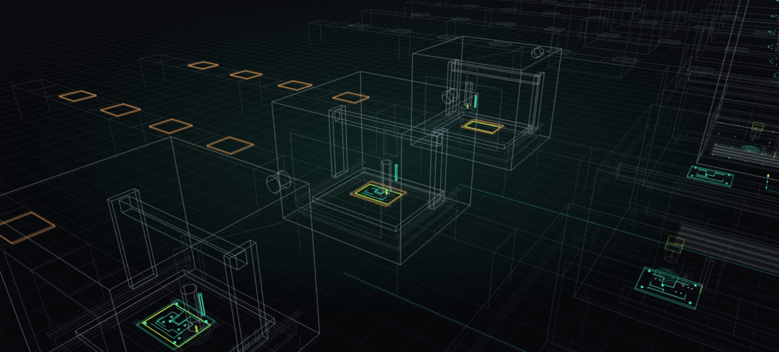
Still image of the simulationConcept simulation
Concept simulation. The continuous transfer between machines shows the vision of the platform, not a capability that has been demonstrated.
01Bench product

Lumaspect Make™

Isolates the traces, drills and cuts a copper-clad panel into a simple lab board.

  1. Copper-clad panel clamped on the bed
  2. Height map of the copper
  3. Trace isolation
  4. Drilling
  5. Outline cutting
  6. Extraction and cleaning

Subsystems

Drag to rotate, scroll or pinch to zoom.

Concept: structure and size to be defined, no drawings yet.

  • Machining with a cutter that removes material, not 3D printing.
  • Containment and extraction of copper and fibreglass dust.
  • Cleaning of the board before assembly.
  • Not included: plated through holes and multilayer boards.
02Data sheet

Data sheet in brief.

The same fields for the four steps, so they can be compared.

  • In the design
  • Target to validate
  • Future option
  • To be defined
Data sheetLumaspect Make™Lumaspect Apply™Lumaspect Reflow™Lumaspect Check™
FunctionTrace isolation, drilling and outline cutting of prototype PCBsTarget to validateSolder paste dispensing and component placementIn the designReflow soldering with a controlled thermal profileIn the design2D optical inspection with AI of assembled boardsIn the design
InputSingle or double-sided copper-clad panelTarget to validateBare clean PCB, components on tape or trayIn the designPCB with paste and placed componentsIn the designSoldered PCBIn the design
OutputPCB without plated holes, to be cleaned before assemblyTarget to validatePCB with unreflowed paste and placed componentsIn the designSoldered and cooled PCBIn the designResult per component (OK, to review), images, recordIn the design
Bench configurationTo be definedTo be definedApply™ L3: 806 × 706 × 451 mm, front drawerIn the designReflow™ L3: 700 × 560 × 340 mm, chamber with drawerIn the designVision™ L3: about 545 × 500 × 310 mm, about 14 kg, front drawerIn the design
Possible in-line integrationTo be definedTo be definedModule of the L3+ mini line (concept); in-line L5 version (design, development on hold)Future optionIndexed chamber of the L3+ mini line (concept); L5 tunnel oven (design, development on hold)Future optionVision™ L4 and L5 in line (designs, development on hold); module of the L3+ mini line (concept)Future option
Work area or board sizeTo be definedTo be defined350 × 250 mmIn the design350 × 250 mmIn the designFrom 50 × 50 to 350 × 250 mmTarget to validate
Main subsystemsX/Y/Z axes, spindle, probe, spoil board, extractionTarget to validateCoreXY, piston dispenser, nozzle with vacuum and rotation, top and bottom cameras, feedersIn the designStainless chamber, heaters above and below, convection, cooling, 4 thermocouples, fume outletIn the designCoreXY with Z, IMX296 camera, 25 mm lens, RGBW ring, Raspberry Pi 5In the design
Design data neededGerber of the traces, Excellon drill file, outline (from KiCad or other CAD)Target to validateBill of materials (BOM), placement file (CPL), paste layer (Gerber); IPC-2581 and ODB++ as a targetTarget to validateProfile for the paste alloy (from the board program)Target to validatePlacement file (CPL) and one good boardIn the design
Power and services230 V; dust extraction required; power to be definedTo be defined230 V; vacuum from an internal pump, no compressed air; power to be definedTarget to validate230 V 10 A; fume extractionTarget to validate100–240 V, 100 W; Ethernet and Wi-FiTarget to validate
Development statusConcept under evaluationIn the designPreliminary design; smallest component 0603 imperial to validateTarget to validatePreliminary design; profile from a model, not measuredTarget to validatePrototype in development; 2D in development, 3D under evaluationIn the design

Values marked “in the design” are set in the drawings but not yet measured on a prototype.

Get news on the prototype and on chances to join the first demonstrations.

Notify me about Make
03In depth

How it works, in detail.

How it works

A cutter removes the copper around the traces until they are electrically isolated; then a drill makes the holes in the pads and a cutter cuts the board outline. It is machining, not printing.

The cutting depth is a few tenths of a millimetre, so the flatness of the panel matters. A probe measures the height of the copper on a grid of points and the machining follows it.

Architecture and subsystems

Gantry with X/Y/Z axes, high-speed spindle with manual or automatic tool change (to be defined), spoil board, probe, extraction shroud and closed enclosure.

Operating flow

Export from CAD → toolpaths → clamp the panel → height map → isolation → drilling → outline → extraction and cleaning → board ready for Apply™.

Integration with the other machines

Make™ would produce the bare board that Apply™ receives. The handover needs cleaning: dust and burrs on the pads spoil the paste and the solder joints. In-line integration is not designed.

Expected input and output formats

Input: RS-274X Gerber of the traces and the outline, Excellon drill file. Output: the board and a machining log (tools, depths, height map). Formats to be confirmed.

Calibration and maintenance

Axis homing, height map on every panel, cutter wear check, spoil board replacement, extractor filter cleaning.

Technical limits and open questions

Not included: plated through holes, multilayer boards, solder mask and silkscreen.

To evaluate: minimum trace and isolation width, minimum component pitch, noise, fibreglass dust (harmful to breathe: extraction is required), tool cost.

For boards with plated holes or several layers, a PCB manufacturer remains the better choice.

Open-source projects

Used in the project

None so far.

Under evaluation

  • FlatCAM · From Gerber files to toolpaths for trace isolation.
  • pcb2gcode · A command-line alternative for the same step.
  • grblHAL · Firmware for the axes of a milling machine.
  • bCNC · Height mapping with the probe (auto-levelling).
04Cheat sheet

The summary to print.

Cheat sheet

Lumaspect Make™

From copper-clad panel to PCB.

Rev. A · 2026-10-12Concept under evaluation
Function
Trace isolation, drilling and outline cutting of simple lab PCBs.
Input → output
Single or double-sided copper-clad panel → PCB without plated holes, to be cleaned.
Operating cycle
Clamping → height map → isolation → drilling → outline → extraction and cleaning
Requirements
Gerber and Excellon from CAD · 230 V · extraction with filter
Limits
No plated holes · no multilayer · dust to contain · minimum resolution to evaluate
Status of the specifications
Concept under evaluation. All values are to be defined.
lumaspect.com/en/make/ · Rev. A · 2026-10-12
Keep me posted

Notify me about Make

Get news on the prototype and on chances to join the first demonstrations.

What are you interested in · required